Semiconductor and display manufacturing increasingly depends on the stability and precision of optical components used in high-energy laser and large-area processing systems. GENERAL OPTICS provides high-performance optical solutions—ranging from ultra-large ELA windows to precision laser optics—designed to enhance yield, reliability, and productivity in advanced display and semiconductor production lines.
Industry Challenges
Modern semiconductor and display processes require:
- Optics capable of withstanding high-energy excimer laser exposure
- Large-area substrates demanding long, high-precision optical windows
- High surface quality and wavefront accuracy for stable annealing performance
- High-reliability coatings with excellent thermal and environmental durability
- Beam shaping and homogenizing solutions for process uniformity
GENERAL OPTICS addresses these challenges with vertically integrated manufacturing, advanced coating technologies, and rigorous quality assurance.
Our Solutions
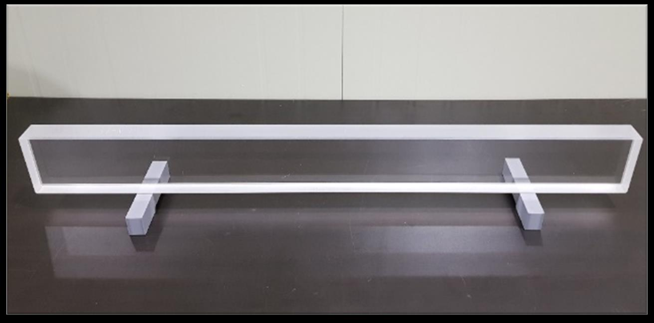
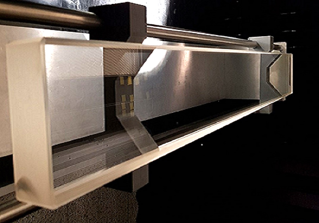
Large ELA Optical Windows
High-energy Excimer Laser Annealing (ELA) systems require long optical windows with exceptional durability and uniformity.
GENERAL OPTICS manufactures fused-silica annealing windows up to:
- Length: 850 mm, 1150 mm, 1200 mm, 1800 mm, and 1850 mm
- Material: High-purity fused silica
- Applications: ELA, LLO, LTPS/oxide TFT manufacturing
These windows are produced using in-house large-diameter polishing machines (up to 1850 mm) to ensure exceptional flatness and surface quality.
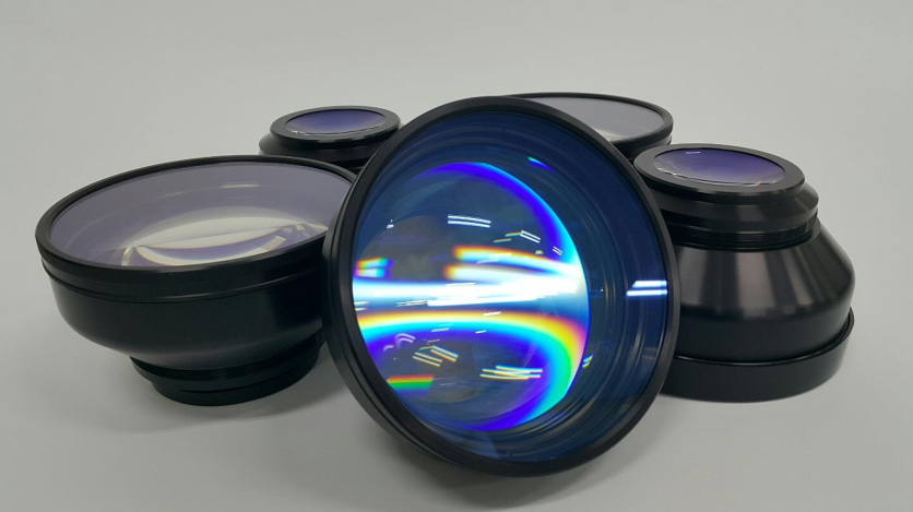
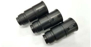
High-Performance Laser Optics for Semiconductor Processes
GENERAL OPTICS provides a broad portfolio of laser optics tailored for semiconductor and display production equipment:
- F-Theta lenses (20+ models)
- Beam expanders (1X–4X)
- Laser collimators (10 models, water-cooled options available)
These optics are engineered for:
- High-power UV/visible/NIR laser processing
- Critical dimension control
- Uniform energy distribution across large panels
- Improved process stability and throughput
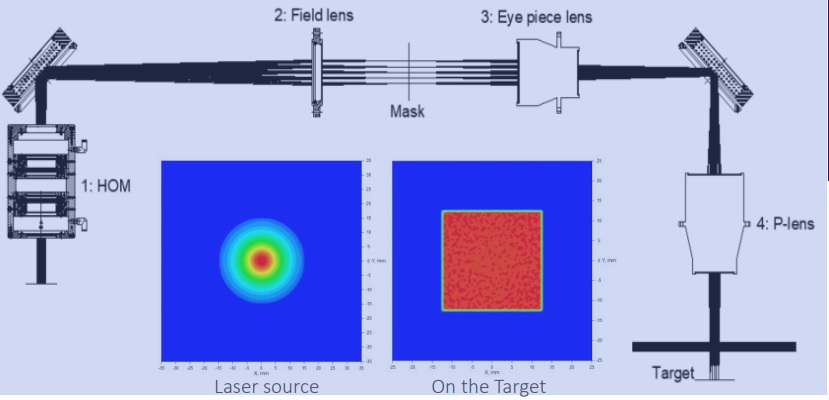
Beam Homogenization Solutions
To achieve uniform annealing and patterning results, laser beam profiles must be precisely controlled.
GENERAL OPTICS offers:
- Waveguide-type homogenizers
- Lens-array homogenizers
- High-uniformity projection optics (measured >97.5% uniformity)
These systems ensure high consistency across large substrates and enhance overall device yield.
Manufacturing & Quality Advantages
Advanced Coating Capabilities
GENERAL OPTICS operates multiple large-format E-beam and IAD coating systems:
- Chambers from Φ900 to Φ2050
- End-Hall and RF-coil ion sources for dense, durable coatings
Optical coatings are tested under MIL-STD durability procedures, including:
- Abrasion
- Adhesion
- Humidity
- Temperature cycling
- Solubility & cleanability tests
This ensures long-term stability in demanding semiconductor fabrication environments.
Precision Measurement & Verification
To guarantee optical performance, GENERAL OPTICS utilizes:
- 4-inch and 15-inch Zygo interferometers for wavefront measurements
- Talysurf PGI Optics for aspheric surface evaluation
- FT-IR and UV-Vis spectrophotometers for transmission/reflection analysis
These capabilities are essential for maintaining the high flatness, surface roughness, and optical uniformity required in semiconductor production optics.
Why GENERAL OPTICS
- Proven experience supplying optical components for major semiconductor and display processes
- One-stop manufacturing: grinding → polishing → coating → assembly → inspection
- Large-format optics production unmatched by typical mid-sized manufacturers
- Certified quality management systems (ISO 9001, ISO 14001)
GENERAL OPTICS delivers the optical precision and reliability demanded by next-generation semiconductor and display technologies.